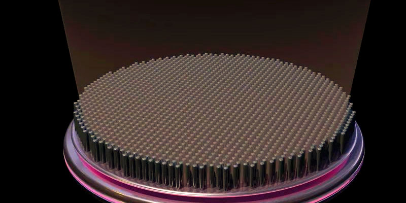
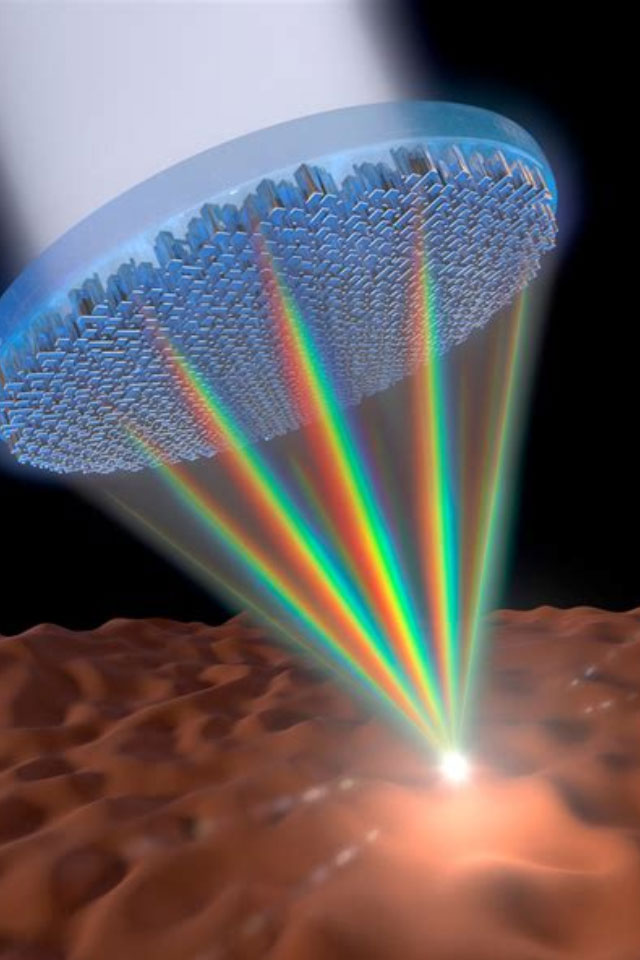
A superlens, an innovative optical element that provides fine control of incident light through a pattern of sub-wavelength “superatoms” on a dielectric surface. These superatoms uniquely alter the phase distribution of the incident beam, allowing for precise bending or redirection of the beam. These tiny nanoscale structures are able to effectively control light interactions due to their different shapes and sizes and their arbitrary position on the lens. Although the term “lens” is often associated with focusing light, superlenses are much more than that and have a wide range of applications, including phase control.
To achieve this fine phase control, a superlens needs to have a significant difference in refractive index, which is largely dependent on its material selection and manufacturing process. Material selection should take into account the target wavelength range of the application, while ensuring that material absorption is minimized and that the manufacturing process meets the feature size requirements. For example, silicon is ideal for near-infrared applications such as LIDAR sensors, while materials such as titanium dioxide, gallium nitride and silicon nitride are suitable for camera applications in the visible wavelength range.
The manufacturing process for the superlens is equally critical. Currently, electron beam lithography has a place in the research arena for its superior precision and versatility, although it is not suitable for mass production. Deep ultraviolet (DUV) lithography, on the other hand, is widely used in semiconductor fabrication, providing critical support for high-resolution patterning. Nanoimprint lithography, on the other hand, stands out for its cost-effectiveness and scalability, opening the way for high-precision nanoscale pattern replication.
However, these fabrication methods have limitations in supporting variations in the Z-axis direction, and thus current superlens designs tend to adopt binary shapes, i.e., maintaining uniformity in the Z-axis while flexibly defining superatomic patterns in the XY plane. In addition, the fabrication process affects material selection, e.g., photolithographic fabrication is suitable for silicon or other materials commonly used in semiconductor fabrication, whereas nanoimprint lithography may use a different type of UV- or thermally curable epoxy.
In summary, fabrication of superlenses faces the challenge of low-cost mass production, which stems largely from their special need to combine small feature sizes for phase control with large sizes for numerical aperture/beam size. While we are still in the early stages of superlens manufacturing, and it is unclear whether certain material systems or manufacturing processes can achieve the economies of scale of the semiconductor and photonic integrated circuit (PIC) industries, the thinness advantage of superlenses may be sufficient to offset their cost challenges in certain applications, such as advanced technologies such as medical endoscopy.
optlenses
Related Blogs


